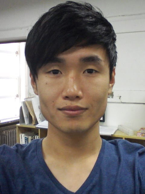
Jungmin Lee (2012)
Dept. of Electronic and Information Engineering Seoul National University of Science and Technology
232 Gongneung-ro, Nowon-gu, 01811, Seoul, KOREA
chukboka naver.com
Education & Experiences
PDE TD PI (Product Development Engineering, Technology Development & Process Integrator), Micron (Located at Taichung).
2012.08, B.S. in Dept. of Electronic and Information Engineering, Seoul National University of Science and Technology.
2011.07, Research Intern, SoC Research Center, Korea Electronics Technology Institute (KETI).
2010.09 - 2012.06, Research Assistant, SoC Platforms Lab., Seoul National University of Science and Technology.
2012.08, B.S. in Dept. of Electronic and Information Engineering, Seoul National University of Science and Technology.
2011.07, Research Intern, SoC Research Center, Korea Electronics Technology Institute (KETI).
2010.09 - 2012.06, Research Assistant, SoC Platforms Lab., Seoul National University of Science and Technology.
Research Interests
- Develop & Study for Mobile hand held Device.
- Human Body Communication.
- Sutdy for Smart Device Application Development Environmint.
- Human Body Communication.
- Sutdy for Smart Device Application Development Environmint.
Projects
- Develop Module for Human Body Communication.
- Develop Environment for Linux Development.
Presentations
- 1 "An Android System Design and Implementation for Telematics Services, " SPL meeting. Mar. 2011.
- 2 "A Location Tracking and Messaging System for Mobile Group Communication in IP Networks, " SPL meeting. Mar. 2011.
Skills
-FPGA prototyping
-EDA tools: ModelSim, HSpice, ORCAD, Quartus, Xilinx ISE
-FPGA Prototyping: Altera, Xilinx
-Analysis Language: MATLAB
-High-level Computer Language: C, C++, Vsual C++
-Microprocessor: Atmega
- Study for Linux Development Environment.
Courses
Circuit Designs, Digital System Design